Etching, which was used for printing and copperplate engraving in ancient times, is still active today as a core technology in the manufacture of printed circuit boards and semiconductors. This section describes the principles and types of etching, and explains how it relates to the cleaning process and what we need to pay attention to when performing etching.
Employed in printing and copper engraving in ancient times, etching even today plays an active role as a key technology in the manufacture of printed-circuit boards and semiconductors. This article sets forth the principles and types of etching, and discusses its relation to cleaning operations, and what cautions must be taken when etching is carried out.
There is a way of working materials that is referred to as “etching.” Seemingly not that well known in general, etching is a type of chemical processing method utilizing the properties of acids, alkalis, and ions. Etching is a technique that nonetheless is extraordinarily often employed in places imperceptible to the eyes. Here we will discuss the principles of etching, the types of etching, and the materials that are subjected to etching.
What is etching?
Etching, one type of the ways that the surface of process-object materials—primarily metals, glass, and semiconductors—is worked, yields target shapes by exploiting the corrosive properties of acids, alkalis, and ions to remove portions of the surface.
Other ways of working a material to obtain target shapes by removing portions of the material include cutting and grinding, but etching is frequently utilized when carrying out processing with accuracy better, and elimination quantity (amount of material removed) more miniscule, than those methods is desired.
Principles of Etching
The principles of etching are first to apply a durable substance called “resist” to areas of the surface being etched that are not to be removed.Carrying out etching in that state removes the areas other than where the resist has been applied.Afterwards, by removing the applied resist, patterns and designs can be formed on the surface of the etched work.
The primitive invention of etching is surprisingly old; that which was invented in Europe around 1500 is said to be the first. Since then, etching has been widely utilized for making printing plates and works of art. Entering the modern era, etching evolved into photoengraving technology that incorporates photographic techniques into platemaking. Current processing of printed circuit boards and semiconductor wafers incorporates further developed versions of this photoengraving technology. In particular, in the manufacture of semiconductor devices, technology known as photolithography, which can be termed the ultimate limit of photoengraving, is employed on the order of nanometers (one billionth of a meter).
An advantage of etching is that processes of higher precision than cutting or grinding may be batched. For this reason, etching is often utilized in the manufacture of printed circuit boards and the processing of semiconductors, and in the process operations of micro-electromechanical systems (MEMS). Put differently, it could be said that the development of printed circuit board manufacturing, semiconductor processing, and MEMS prompted the development of etching technology.
In contrast, etching is not very suited to processes for which the amount to be removed is large. Etching basically is a process on the scale of slightly shaving surfaces. Consequently, desiring to process material into three-dimensional shapes by removing more significant portions from the material requires looking into different processing methods.
Also, as set out below, in etching there are systems of two kinds: With wet etching, which employs acidic and basic solutions, thought must be given to waste-liquid disposal. Likewise, with dry etching, in which etching is carried out by ion-beam bombardment, since a vacuum chamber is necessary, the fact that the equipment will a large-scale project must be taken into consideration.
Categories of Etching
Wet Etching and Dry Etching
Etching is grossly divided into two techniques. One is wet etching, which exploits the corrosivity of both acidic and basic solutions to remove material. Wet etching is employed widely in such applications as printed wiring boards, glass decoration and processing, and copper engraving, and may also be used as an adjunct in semiconductor processing and MEMS processing.
The other is dry etching, in which processing is carried out by removing atoms in the surface of the work by means of an ion beam. The impression is close to a sense that the ionized particles strike the surface of the work at high speed, sending the atoms in the work surface flying. Dry etching is primarily used for semiconductor processing and MEMS processing. In recent years, with ion-beam output power on the rise, dry etching has begun being applied to processes in which the removal volumes are large.
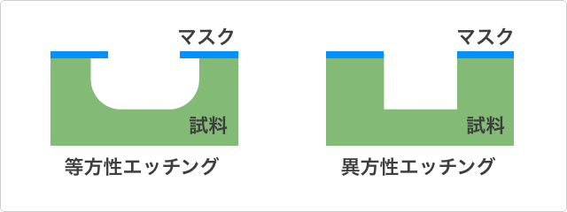
Isotropic Etching and Anisotropic Etching
In wet etching, furthermore an important distinction is that between isotropic etching and anisotropic etching.
Isotropic etching means that etching reactions heading in all directions take place. For example, if the etching reaction starts in an area of the surface of the work near the resist, what happens is that a reaction proceeds in which corrosion, advancing in all directions, enters beneath the resist, gouging the bottom of the resist. This is sometimes called “undercutting.” In this case, when the etching finishes and a cross-section of the work is viewed, it will have been processed into a U-shape or, rotated 90 degrees sideways, a C-shape, with rounded edges. Isotropic etching happens if the reaction rate is fast.
Anisotropic etching enables edge-defining processes to be carried out but will not occur unless the reaction rate is slowed down.
That is, whether isotropic or anisotropic is determined by the etching reaction rate. In order to control the reaction rate, a combination of such factors as the concentration, type, and temperature of the etching solution, and stirring of the solution is critical.
Mechanism Whereby Isotropic/Anisotropic Etching Occur
Taking a brief look at the etching reaction in microscopic terms, the mechanism whereby isotropic and anisotropic etching occur depends largely on the crystalline structure of the surface of the material etched. For example, when a silicon material is etched with hydrofluoric acid, the etching should be isotropic. Yet whether the etching is isotropic or anisotropic is determined according to which crystal plane, in a cross section through the crystalline lattice constituting the silicon material, appears on the surface. The etching will be isotropic if among the atoms constituting the crystalline lattice, the number of atoms that appear on the surface is large, and will be anisotropic if the number is small.
Furthermore, the strength of crystalline lattice bonds, that is their “permissiveness” to etching, depends on the type of elements that compose the material etched. For example, compared with copper, silicon is less permissive of etching, and requires a strong acid such as hydrofluoric acid. Thus, in general, the etching will be isotropic when a powerfully reactive strong acid is employed, and will be anisotropic when a weakly reactive acid is employed.
Moreover, in some cases a surfactant is added to the etchant, wherein the production of isotropic or anisotropic etching can be controlled according to the type and concentration of the additive.
In reality, carrying out the etching as an anisotropic process is desirable in order that the edge-defining patterns be satisfactory, but inasmuch as the reaction rate must be lowered, the efficiency will be poor. Conversely, attempting to raise the process speed will lead to isotropic etching and end up giving rise to undercut. How to overcome this apparent contradiction can be said to be the skill of etching engineers and technicians.
Isotropic Etching and Directional (Vertical) Etching
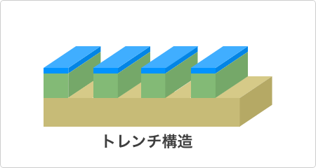
Meanwhile, dry etching is categorized into isotropic etching and directional (vertical) etching, with the usage being divided according to the purpose. Dry-etching isotropic etching corresponds to the isotropic etching of wet etching, while dry-etching directional etching corresponds to the anisotropic etching of wet etching. Directional etching, in particular, is a technique that has developed in recent years and is often utilized when it is necessary to carve minute deep holes, called trench structures, in silicon wafers. In the case of dry etching, these structures are controlled by the combining of ion-beam intensity and type of ions (type of atomic element), among other factors.
The foregoing is the basic theories of etching reactions, but in actuality, these different reactions may occur simultaneously; there are many poorly understood aspects to the phenomena that occur in the course of etching reactions. In many cases, the work proceeds not only on the basis of these theories, but also on field experience and knowhow gained through repeating many trial manufactures and experiments.
Therefore, specific and detailed information such as the composition, concentration, and processing time of an etchant is each enterprise’s secret. In particular, it is usually the case that semiconductor-wafer etching and cleaning processes are vital, confidential information.
Material to Be Etched
Examples that may be given of principal materials that are the object of wet etching are such metals as copper and iron, and semiconductors such as silicon. And by utilizing extraordinarily strong acids and such as aqua regia and hydrofluoric acid, or strong bases, glass and ceramics can be the object of wet etching as well. In the case of dry etching, while metals also are an object of the process, the principal object is silicon and other semiconductors.
As for specific applications, with wet etching, patterned layer formation on printed-circuit boards is overwhelmingly common. Wet etching is also utilized in the microscale processing of metals and ceramics, and in the fine arts, in the fabrication of printing plates for copper engraving. With dry etching, examples that may be given include the processing of semiconductor wafers and the fabrication of MEMS.
Composition of Etchant and Waste-Liquid Disposal
The essentials when wet etching is carried out are the etchant and its disposal. First, let’s take a look at etching on copper.
For etching copper, ferric chloride (FeCl₃) is mainly used. When copper is placed into an aqueous solution of ferric chloride, the copper dissolves out into the solution. Then, the iron and copper interchange, producing copper chloride (CuCl₂). While these are the principles of chemical etching, since copper chloride is toxic, the Pollutant Release and Transfer Register (PRTR) regulations (laws relating to the promotion of reforms in comprehending and managing the volume of discharge into the environment of designated chemical substances) strictly restrict the discharge of copper chloride into the environment. In other words, if it is not rendered nontoxic, copper chloride cannot be flushed into the sewer.
This mandates disposal-treating the waste liquid. Specifically, hydrated lime (calcium hydroxide: Ca(OH)₂) is put into the waste liquid to decompose it into copper hydroxide (Cu(OH)₂) and calcium chloride (CaCl₂). Furthermore, when heated, copper hydroxide decomposes into copper oxide (CuO) and water (H₂O). Calcium chloride and copper oxide are harmless, and in that state can be flushed down the drain. These are the chemical principles of etchant waste-liquid disposal.
Likewise, hydrofluoric acid (chemical formula: HF) is used for wet etching carried out on glass and silicon, but is a highly toxic substance that requires careful handling. For that reason, it is critical that waste hydrofluoric-acid solution also be disposal-treated. Common with disposal-treatment of hydrofluoric-acid waste solution is a technique of reacting it with hydrated lime or calcium chloride to produce calcium fluoride (CaF₂). Calcium fluoride is harmless and can be flushed down the drain.
In any of these instances, the essence of the wet etching process and disposal-treating of the waste solution is chemical reactions. Thus, diverse acids and bases are employed. Many of these chemical products are harmful to the ecosystem and the human body, and so their handling on the job and in disposing of the waste solutions is extremely important.
Wet Etching Process
In general, wet etching on etching-material plates is carried out by process steps along the lines of the following.
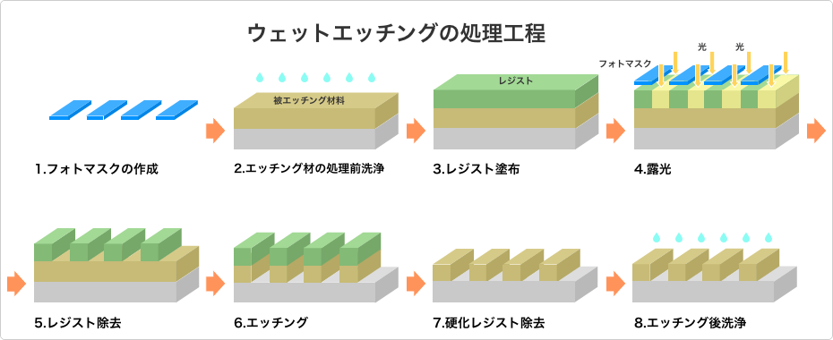
- Creation of Photomask: The pattern to be processed is drawn on a transparent sheet. In the majority of cases, resists are cured by ultraviolet rays, and so basically the pattern is drawn to shield areas that are not to remain.This means, in other words, that a “negative” is created.
- Pre-Treatment Cleaning of Material Etched: The surface of the material being etched is scrubbed to remove excess oil and debris. This enables the photomask and photoresist to be set evenly on the work. It also is effective to reduce post-etching residuum.
- Application of Photoresist: A photoresist is applied to the material being etched. Ordinarily resists harden in response to ultraviolet rays, so the application is carried out in an environment where ultraviolet rays don’t enter. And since some resists are highly toxic, care in handling is mandated. Some resists, however, function in sheet form, in which case the resist is stretched over the material being etched to cover it as a sheet.
- Exposure: On top of to-be-etched material onto which a photoresist has been applied, a photomask is set and is exposed to UV rays. This cure-hardens and imparts acid resistance to the areas of the resist other than where it has been marked with the photomask.
- Removal of Photoresist: The resist apart from the hardened areas is washed off.
- Etching: Etching is carried out. This corrodes the surface apart from the hardened areas, transferring onto the work surface the pattern marked with the photomask.
- Removal of Hardened Photoresist: The cure-hardened resist is removed. Chemicals specified by the photoresist manufacturer are employed.
- Post-Etch Cleaning: A final cleaning is performed. This will remove any remaining etchant or residuum.
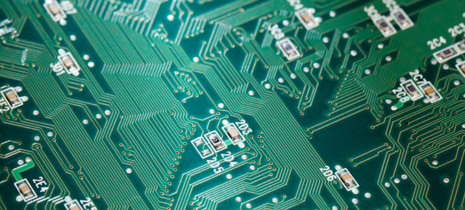
The foregoing are the general process operations for wet etching. For printed-circuit boards, wet etching is followed by the application of solder mask and the formation of through holes. Also, for multilayer boards, there are further operations including a laminating compression process; in some cases the number of process steps may amount to from 30 to 50 steps.
→ Article “Printed Circuit Boards and Etching: An Overview of Etching on Printed Circuit Boards”
Cleaning after wet etching is indispensable. If cleaning is neglected, components of the etchant will remain on the work and become a source of corrosion and rust. Moreover, if printed circuit boards are not cleaned sufficiently, remaining etchant components will corrode the patterned conducting lines, causing conductor breakage or other faults. Especially in the case of multilayer boards, after laminating compression has been applied to a board, it can neither be visually inspected nor cleaned. Therefore, it is necessary to thoroughly clean the substrates individually, while they are in an independent state before being subjected to laminating compression.
Furthermore, with wet etching equipment and cleaning equipment being quite similar structurally, they share a deep connection. Some etching devices are manufactured incorporating a cleaning function, some sharing an etching tank with a cleaning tank, or conversely, some cleaning devices are manufactured incorporating a simple etching function.
What’s more, cleaning is necessary even after dry etching. Cleaning in the semiconductor manufacturing industry is referred to as “atomic cleaning” and is performed to remove unwanted atoms from the work surface. The purpose is to clear away residuum generated by dry etching, to remove tiny dust specks that cannot be seen with the eyes, as well as to keep the semiconductor junction surfaces clean.
Cleaning operations are frequently required at key points in the etching process, regardless of whether the etching is wet or dry. And because the types of chemical solutions required are numerous and a large amount of chemical solutions is consumed, thought must be given to waste-liquid disposal treatment of the chemicals.
In addition, special chemical solutions called parting agents are employed when the removal of photoresists and cure-hardened resists is carried out. Since depending on the type, some resists are toxic, thought must also be given to waste-liquid disposal treatment of these chemical solutions.
Measures for Dealing with Fluids Remaining from Cleaning and Recommendations for Moisture-Absorbing Rollers
Cleaning is divided into a washing operation employing chemical solutions, a rinsing operation to remove the chemical solutions post-wash, and a drying operation. For the cleaning operation batch processing and single-wafer processing systems exist, with the usage being divided according to the application. In batch processing, the processed object is immersed in a cleaning tank filled with a chemical solution. In some cases, the cleaning solution is subjected to physical vibration by means of ultrasound, and the cleaning solution may also be stirred at the same time. In single-wafer processing, cleaning of a processed object is carried out by spraying cleaning solution onto the article, after which the cleaning solution is thoroughly removed in the rinsing operation.
What is important is “liquid draw-off” to get as much residuum and leftover etchant from up through the etching operation cleared away as possible prior to going into the washing operation. This is because if the liquid draw-off is not sufficient, residuum and etchant from up through the etching operation can get mixed into the cleaning solution in the cleaning operation, degrading the cleaning power of the cleaning solution and shortening its service life.
After the washing operation the work enters the rinsing operation, wherein liquid draw-off post-washing-operation and post-rinsing-operation are also important. If liquid removal is not sufficient post-washing-operation or even post-rinsing-operation, the likelihood that faults such as water marks will occur in the product will be high. Also, in consideration of the environment, for the rinse solution purified water has begun to be utilized in recent years in place of organic solvents and chlorofluorocarbons. Purified water features a higher boiling point, making it unlikely to volatilize at room temperature. Therefore, carrying out liquid draw-off sufficiently during the washing and rinsing operations is necessary to reduce the burden on the subsequent drying operation.
For the drying operation, in the case of dry etching, especially drying with respect to semiconductor wafers liquid draw-off by means of centrifugal force from spinning the wafers is the common practice. On the other hand, in wet etching, common practices include drying by heat and liquid draw-off by means of air nozzles, but heat and air-nozzle mediated drying consume relatively large amounts of electricity, there is a likelihood of their having some sort of adverse effect on the processed object due to the heat. Other disadvantages are that the noise from air nozzles is loud, and that heaters for thermal drying and compressors to generate the compressed air that the air nozzles use are required, leading to higher facilities costs.
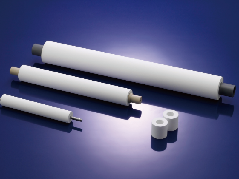
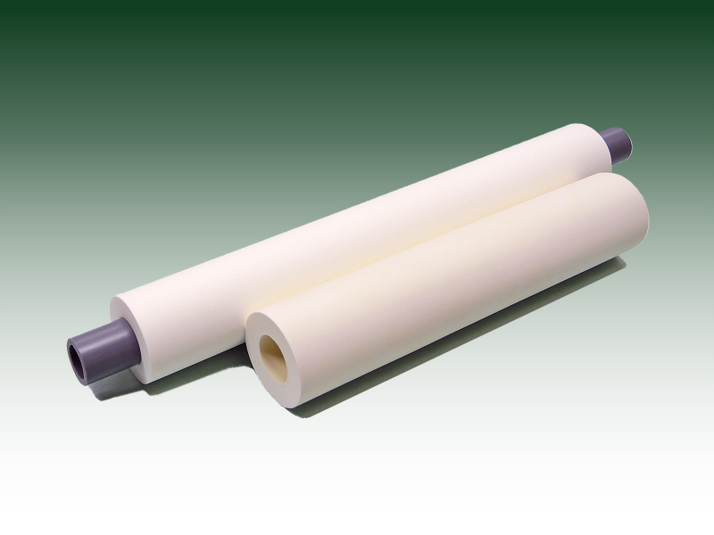
The Option of Utilizing Moisture-Absorbing Rollers
Against this backdrop, it would be a good idea to consider putting water-absorbing (liquid-absorbing) rollers to work, especially when the processed objects are of planar form. Moisture-absorbing rollers, rollers in the form of porous rolls made out of synthetic resin, are designed to contact, while applying a certain amount of pressure to, the surface of a processed object to soak up moisture from the object.
And of late, moisture-absorbing rollers that have chemical resistance to strong acids and bases are also available, enabling adequate handling of liquid draw-off of etchants employed in wet etching processes. Moreover, many of these rollers are endowed with enhanced moisture absorbency and outstanding elasticity, making it possible to lessen to the absolute minimum the chance that fluids remain from the etching and cleaning operations.
In particular, the proven successes of the rollers in wiping off printed circuit boards, lead frames, and glass plates have been on the rise. In addition to that, moisture-absorbing rollers also have advantages from a cost perspective. One is that they keep power consumption in the drying operation in check. Furthermore, since the moisture-absorbing rollers are simply installed at the outlet of the cleaning device or etching device, liquid draw-off can be carried out with no providing of complicated equipment
—another reason the rollers tie in to curtailing equipment costs. Not only that, but providing moisture-absorbing rollers increases the efficiency of moisture and chemical removal, so that their carryover into subsequent processes can be kept under control.
Moisture-absorbing rollers: playing an active role in liquid draw-off of the chemicals indispensable in wet etching.
Thus we have taken a broad look at etching methodology. In wet etching, preventing the etching solutions from being carried over into subsequent operations, and waste-liquid disposal treatment are crucial. Moreover, following the etching operations, cleaning is mandated. While cleaning operations cannot be omitted, carrying out liquid draw-off with moisture-absorbing rollers rather than using air nozzles and heat makes it possible to configure the facilities more simply. Accordingly, improvement in product reliability and lowering of facility operating costs can be expected.