Printed-circuit-board technology is technology that electronic devices cannot do without. Its very existence supports modern technical means, but when it comes to "printed circuit boards," there are various differences. Here we describe the types of printed circuit boards, and we also explain printed-circuit-board manufacturing operations and design considerations.
The creation of printed circuit boards is inextricably linked with the etching process. The question of how a printed circuit board will turn out is up to the quality of the etching process. Here, we will explain printed-circuit-board types and printed-circuit-board pattern formation methods, as well as processing procedures and things to note when ordering from a vendor.
What are printed circuit boards?
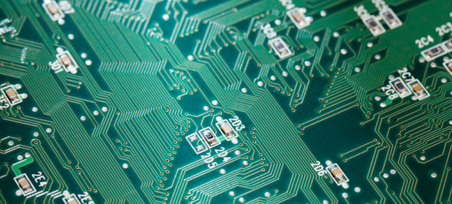
If you open a personal-computer case, you can see that installed inside, along with the power-supply unit and cooling fan, is a motherboard on the surface of which numerous electronic components are mounted. These motherboards are generally referred to as “printed circuit boards.”
Printed circuit board technology is one of the core technologies indispensable for modern electronic devices, and is almost always used in modern electronic devices such as LCD TVs and mobile phones.
History and Basic Structure of Printed Circuit Boards
A single-sided board that appeared in the 1940s is said to be the first printed circuit board. Since then, in accordance with the growing complexity and sophistication of electronic devices, printed-circuit boards have evolved into double-sided boards and multilayer boards. These days, in answer to high-frequency circuits alumina boards have also appeared, supporting current sophisticated electronic-device technology.
With printed circuit boards, copper foil is stretched onto a base-forming board of paper, resin, or ceramic. Then forming a desired pattern by etching-mediated removal of the copper foil to leave only the required configurational features constitutes the fundamental printed-circuit structure and manufacturing mode.
Types of Printed Circuit Boards
With boards too there are diverse categories. Let’s take a look at their respective differences and characteristics.
Rigid Boards and Flex Boards
Rigid boards are printed-circuit boards whose patterns have been formed onto a hard base plate, meaning they cannot be bent. Generally speaking, “printed circuit boards” are tantamount to rigid boards. While rigid boards cannot be bent, being instead more highly durable and lower cost than flex boards, they currently are the mainstream.
Flex boards are printed-circuit boards whose patterns have been formed onto a pliant synthetic resin polymer. Although they can be bent, flex boards are expensive and compared with rigid boards are less durable. They are mainly used in moving parts or in situations where, with little space in which to sink a board, the board must be folded for packaging.
Single-Sided Boards, Double-Sided Boards, and Multilayer Boards
Single-sided boards are printed circuit boards whose patterns are arranged on only one side of the board. They have the most history and are the fundamental printed circuit board, but are not cut out for complex electronic circuits. Nevertheless, they are often used by amateurs whose hobby is assembling electronic circuits.
Double-sided boards are printed circuit boards whose patterns are arranged on either side. Historically they appeared subsequent to the single-sided board, and they can handle complex electronic circuits to a certain extent. Double-sided boards, however, require being furnished with holes known as “through-holes” as electrical wiring connecting the two sides. Through-holes are holes drilled through a board and into which solder is poured to connect one side of a double-sided board to the other side, and are an essential technology for double-sided boards and multilayer boards.
Multilayer boards, which are the current mainstream, are circuit boards created by preparing multiple double-sided boards, and compressing and bonding the multiple double-sided boards together. Handling complex electronic circuits with these multilayer boards is the general practice. The situation with multilayer boards is that they are manufactured by etching out the patterns layer by layer, after which the layers are laminated, so it is essential that there is no misalignment when the layers are laminated. Since laminating precision, in other words, is called for, the manufacturing of multilayer boards demands sophisticated technology.
Bakelite® Boards, Paper Epoxy Boards, Glass Epoxy Boards, and Alumina Boards
There are also classifications of boards dividing them by the stock material of the base. For Bakelite boards, a phenolic resin impregnated into paper is made the board’s base. They are inexpensively priced, but have poor high-frequency characteristics and low mechanical strength. Bakelite boards are known for being often used in low-cost electronic devices.
For paper epoxy boards, epoxy resin impregnated into paper is made the base. In an earlier era, they were the mainstream. Paper epoxy boards are priced for having better high-frequency characteristics than Bakelite boards, but they are not used much anymore, since glass epoxy boards are the current mainstream.
Glass epoxy boards, glass cloth impregnated with epoxy resin, are the current mainstream. Their cost has become considerably lower than it used to be, and boards of glass epoxy have better high-frequency characteristics than those of paper epoxy resin.
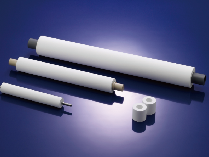
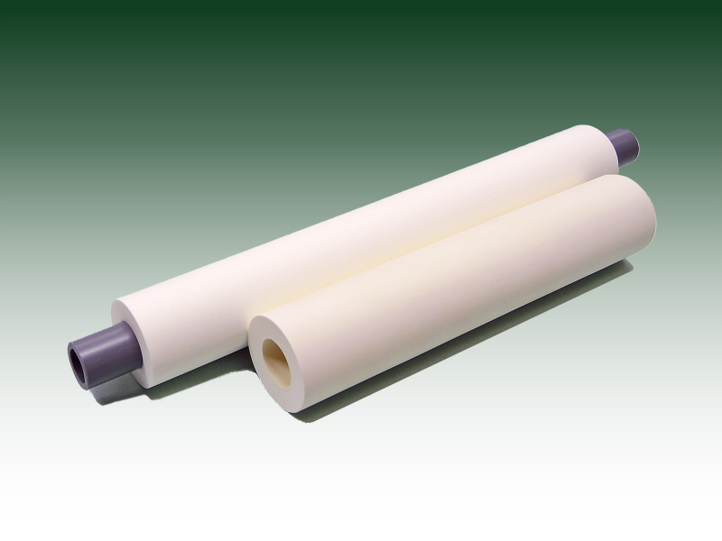
Alumina boards are boards in which a ceramic is made the base, and thus they excel in high-frequency characteristics and heat-dissipation capacity. While a disadvantage is that they are high-cost, their distinctive features are taken advantage of in alumina boards being employed as the principal substrates for high-frequency, high-power circuits.
Other than these categories, there are Teflon® boards that employ a fluoropolymer as the board’s base.
Differences According to Pattern Formation Process
The conventional patterning method is referred to as a subtractive process. In this method, a printed circuit board with copper foil stretched over the entire board surface is prepared, and the unrequired zones are etched to form a pattern. Meanwhile, there is also a special method referred to as the additive process—a method in which the required zones are plated to form the pattern.
Printed-Circuit-Board Manufacturing Stages
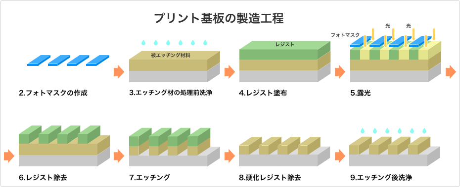
The broad stages of creating a printed-circuit board are as follows.
- Substrate Material Cutting: Green panels that will be the substrate material are cut to a given size. In cases where the board size is small, since numerous boards are processed at once, in order to facilitate post-completion slicing, rows of tiny holes are drilled in the boards or slits are made in them.
- Create the photomask: Create the photomask. In the case of multi-layered boards, create a photomask for each layer. In recent years, patterns are designed using computers, so it is not as difficult as it used to be, but if the rules for design are not followed properly, the finished product will be defective, so care must be taken.
- Cleaning Prior to Substrate Material Etching: The surface of a panel that will be the substrate material is cleaned. This removes invasive grime and makes the resist spread on well.
- Application of Resist: Photoresist is applied to the surface of the panel. Some resists, however, function in sheet form, in which case the resist is stretched over the material being etched to cover it as a sheet.
- Exposure: The created photomask is placed onto the panel surface and optically exposed. Ordinary photomasks are marked so that the areas where the copper foil is to remain are permeated by light. Photoresist cure-hardens when light strikes it, and since the resist will stop the advancement of etching, cure-hardened resist is left atop the copper foil that it is desired remain behind.
- Removal of Resist: Resist that has not cure-hardened, that is, the resist in the areas to be etched, is removed.
- Etching: Etching is carried out. The process etches the areas from which the resist has been removed, while the areas of cure-hardened resist remain.
- Removal of Hardened Resist: The cure-hardened resist is stripped off using a dedicated remover.
- Cleaning: The board displaying the pattern is cleaned to clear away residuum and debris.
- Solder Mask Application: Solder mask is applied to the places where being spattered with solder would be harmful. In the instance of multilayer boards, the solder mask acts as an interlayer insulating layer. Also, in case of multilayer boards, the foregoing 3. through 10. are carried out per board layer.
- Compression Bonding: In the case of multilayer boards, the per-layer panels are laminated, compressed, and bonded together. Crucial at that point is the lamination precision; if the precision is insufficient, defects in the board will arise.
- Through-Hole Formation: Through-holes are formed in interlayer connection locations. Holes are drilled in given locations in the compressed and bonded panel, which is then plated with copper.
- Solder Plating: The panel is given a finish of solder plating to improve component solderability.
- Cleaning: Final-stage cleaning is carried out.
- Inspection: Electrical and visual inspections of the boards are caried out.
Precautions in Designing Printed Circuit Boards
The following three points are representative of what to be careful of when a printed circuit board is designed.
Ensuring Sufficient Clearance between Pattern Lines
If the distance between pattern lines is too close, etchant will be kept from entering between the pattern lines, and as a result, correct pattern formation won’t be possible.
Avoiding Sharp Corners and Infinitesimal Shapes; To the Utmost Not Fashioning Microscopic Gaps
The presence of sharp corners, infinitesimal shapes, and microscopic gaps would be a cause of short circuiting and conductor breakage. Patterns with sharp corners would lead to the problem of photoresist on the corner tips being liable to peel off during etching and hopping off elsewhere.
Not Making the Slits Too Narrow
Slits, which are cuts for snap-splitting printed circuit boards, are processed using a router bit as an end mill of a sort. In the era when panel substrate materials were soft, slender router bits for cutting narrow slits were acceptable, but nowadays harder panel substrate materials are the mainstream. Consequently, bits that are too slender are likely to snap during use.
For Successful Creation of Printed Circuit Boards
This has been an overview of printed circuit boards, and has described stages of their manufacture and considerations to heed in their design. In this article, three considerations to be cautious of in designing circuit boards were noted, but in actual design there are many more cautionary and highly technical issues taken into consideration. Each manufacturer has its own forte depending on its cumulative knowhow, so careful thought should be given to choosing a good supplier.
→Article “Etching: A Processing Method Exploiting the Corrosive Properties of Widely Used Acids”